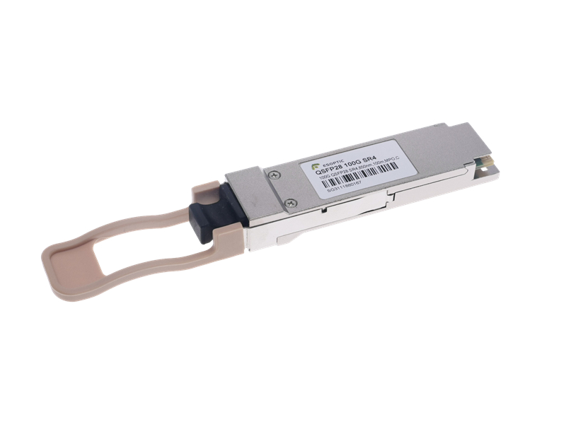
In today’s rapidly advancing optical communication industry, Chiplet packaging technology is becoming a game-changing force in the evolution of optical modules. As data centers scale from 400 G to 800 G and beyond, power density, cost, and bandwidth challenges are driving a new paradigm. At ESOPTIC, we are actively exploring how Chiplet packaging technology can redefine the structure, efficiency, and performance of future optical modules.
The Core Value of Chiplet Packaging Technology
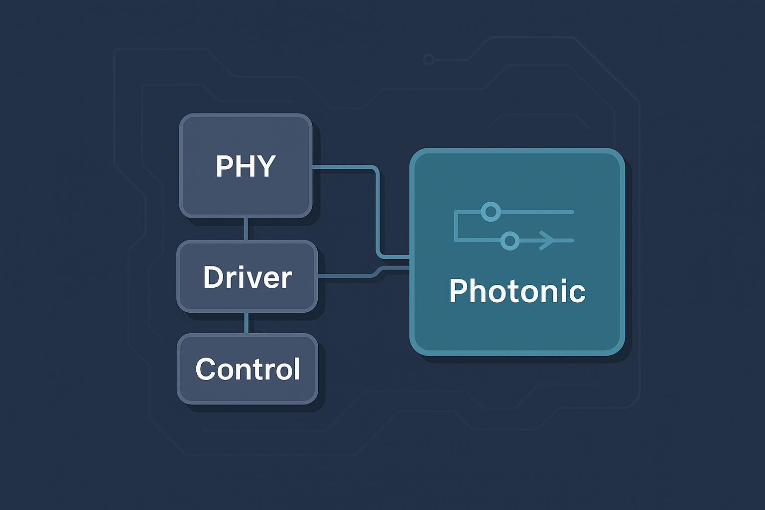
Traditional optical modules rely on large monolithic chips that integrate all functions on a single die. However, as process nodes shrink and complexity grows, such monolithic designs face serious challenges in yield, scalability, and thermal control. Chiplet packaging technology offers a new approach: dividing complex systems into smaller, functional chiplets—such as DSPs, drivers, photonic ICs, and control units—and then assembling them through advanced 2.5D or 3D integration.
For optical modules, this modular method allows for tighter photonic–electronic integration, shorter interconnects, and lower power consumption while maintaining high-speed performance. The result is a smaller, more efficient, and cost-effective module ideal for next-generation data centers.
Key Trends in Chiplet Packaging for Optical Modules
Heterogeneous Integration – The combination of photonic and electronic chiplets enables compact layouts and flexible design. ESOPTIC integrates silicon photonics, drivers, and control ASICs within advanced packaging structures to achieve ultra-high-speed optical performance.
Power and Thermal Optimization – By placing optical chiplets close to processors, Chiplet packaging technology reduces interconnect length and signal loss, achieving better thermal balance and lower total power per bit.
Modularity and Scalability – Each chiplet in an optical module can be upgraded independently, accelerating product iteration and enhancing flexibility for customized optical interconnects.
Advanced Manufacturing – Techniques such as 2.5D interposers, 3D stacking, TSVs, and fan-out wafer-level packaging are essential enablers of chiplet-based optical modules.
Co-packaged Optics (CPO) – One of the most promising applications of Chiplet packaging technology, CPO places optical engines directly beside the switch ASIC, minimizing electrical loss and pushing the limits of optical interconnect efficiency.
ESOPTIC’s Perspective
At ESOPTIC, we view Chiplet packaging technology as the foundation for the next era of optical modules. Our engineering team adopts a system-level design strategy—partitioning optical engines, drivers, and control logic into independent chiplets and integrating them through high-precision packaging processes. This not only enhances reliability and manufacturability but also aligns with the future of high-speed data center and HPC environments.
Future Outlook
The integration of Chiplet packaging technology and optical modules will continue to accelerate as demand for 1.6 T and higher-speed solutions grows. Data centers will benefit from greater density, lower power consumption, and improved scalability. ESOPTIC is committed to developing chiplet-based optical transceivers that deliver exceptional bandwidth and performance while ensuring long-term reliability.
FAQ
1. What is Chiplet packaging technology?
It is a method of dividing large chips into smaller functional dies (chiplets) and integrating them within a single advanced package to improve yield, flexibility, and performance.
2. Why is Chiplet packaging important for optical modules?
It allows photonic and electronic components to be tightly integrated, improving bandwidth, efficiency, and thermal management.
3. What advantages does Chiplet packaging bring to ESOPTIC’s optical modules?
Higher density, modular scalability, lower power consumption, and easier manufacturing upgrades.
4. What challenges exist in adopting this technology?
Thermal design, chiplet alignment, signal integrity, and supply-chain complexity are among the main challenges.
5. How is ESOPTIC implementing Chiplet packaging technology?
ESOPTIC collaborates with packaging foundries to integrate photonic and electronic chiplets through 2.5D/3D assembly, ensuring high-speed, low-loss optical performance for 800 G and future 1.6 T modules.
Conclusion
Chiplet packaging technology marks a transformative moment for optical modules. It enables higher bandwidth, lower power, and smarter integration—all essential for next-generation connectivity. By embracing this technology, ESOPTIC continues to lead in optical innovation, empowering global data centers with faster, greener, and more intelligent optical interconnect solutions.
